 QYC 기판
What are High Frequency PCBs?
Others High Frequency PCBs Manufacturer.A high-frequency PCB manufacturer specializes in producing printed circuit boards designed for applications requiring high-speed signal transmission and minimal signal loss. These manufacturers employ advanced materials and technologies to create PCBs that operate effectively at elevated frequencies, ensuring signal integrity and performance. Their expertise encompasses various types of high-frequency PCBs, including those used in telecommunications, 레이더 시스템, and high-speed digital devices, making them essential for cutting-edge electronic applications.

기타 고주파 PCB 제조업체
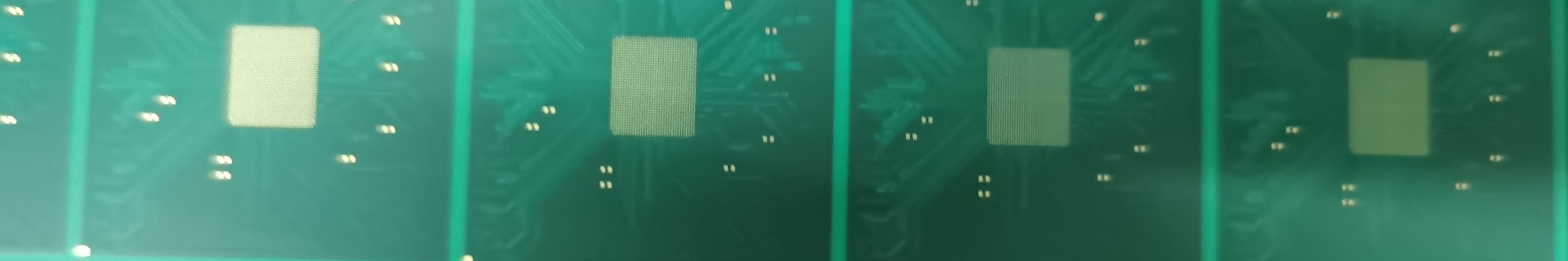
High Frequency PCBs (HF PCB (폴리염화비페닐)) are specialized printed circuit boards designed to handle high-frequency signals, typically in the range of 500 MHz to several GHz. These PCBs are essential in applications where signal integrity and minimal signal loss are crucial, such as in telecommunications, 항공 우주, 군, and high-speed computing.
High-frequency signals can be significantly affected by the dielectric properties of the 폴리염화비페 재료, 신호 경로 레이아웃, and environmental factors. 그러므로, HF PCBs are made from materials with low dielectric constants (디케이) and low loss tangents (디에프) to ensure minimal signal attenuation and distortion. Common materials used for HF PCBs include PTFE (Polytetrafluoroethylene), Rogers materials, and specialized high-frequency laminates.
The Types of High Frequency PCBs
High Frequency PCBs come in various types and configurations to meet the diverse needs of different applications. Some of the most common types include:
Single-Layer HF PCBs: These PCBs have a single conductive layer and are suitable for simple high-frequency circuits such as antennas and low-noise amplifiers. They offer easy fabrication and lower cost but limited functionality.
Multilayer HF PCBs: These PCBs consist of multiple layers of conductive materials separated by insulating layers. Multilayer HF PCBs are used in more complex applications where multiple high-frequency circuits need to be integrated into a compact space. They offer higher functionality and improved performance but are more complex to manufacture.
Hybrid HF PCBs: Hybrid HF PCBs combine high-frequency materials with traditional PCB materials to achieve specific performance characteristics. 이 접근 방식을 통해 설계자는 고주파 성능과 비용 효율성을 위해 PCB의 여러 섹션을 최적화할 수 있습니다.
Flex and Rigid-Flex HF PCBs: These PCBs offer flexibility in design and are used in applications where the PCB needs to be bent or folded. They are commonly used in aerospace, 의료 기기, 그리고 웨어러블 전자 제품.
The Advantages of High Frequency PCBs
High Frequency PCBs provide several advantages that make them indispensable in advanced electronic applications:
Superior Signal Integrity: HF PCBs maintain signal integrity by minimizing signal loss and distortion. This is crucial for high-speed data transmission and reliable performance in communication systems.
Low Dielectric Loss: The materials used in HF PCBs have low loss tangents, which reduce signal attenuation and ensure high-frequency signals can travel longer distances without degradation.
높은 열 안정성: HF PCBs exhibit excellent thermal stability, allowing them to maintain performance and dimensional stability under high-temperature conditions, which is essential for high-power applications.
Mechanical Strength: These PCBs offer robust mechanical properties, enabling them to withstand the physical stresses encountered during assembly and operation.
Compatibility with Advanced Manufacturing Processes: HF PCBs are designed to be compatible with modern manufacturing processes, including automated assembly and high-precision fabrication techniques.
How to Design a High Frequency PCB?
Designing a High Frequency PCB requires careful consideration of various factors to ensure optimal performance. Here are the key steps in the design process:
Choose the appropriate high-frequency material based on the application requirements. Consider factors such as dielectric constant, loss tangent, 열적 특성, and mechanical strength.
Maintain precise control over the impedance of transmission lines to ensure signal integrity. 전자기 시뮬레이션 소프트웨어를 사용하여 PCB 트레이스의 임피던스를 모델링하고 검증합니다..
고주파 신호 경로의 길이를 최소화하여 신호 손실 및 간섭 감소. Use differential pair routing for high-speed differential signals to minimize crosstalk and electromagnetic interference.
안정적인 작동을 보장하고 소음을 최소화하기 위해 견고한 접지 및 배전 네트워크를 설계하십시오.. Use ground planes to provide a low-impedance path for return currents.
효과적인 열 관리 전략 통합, 열 비아 및 방열판과 같은, 고출력 부품에서 발생하는 열을 발산하고 안정적인 작동을 유지합니다..
PCB 설계가 표준 제조 공정과 호환되는지 확인. PCB 제조업체와 긴밀히 협력하여 설계 매개변수 및 제조 능력을 확인합니다..
Why Use High Frequency PCBs Over Other Boards?
High Frequency PCBs offer distinct advantages over traditional PCBs in specific applications:
HF PCBs are designed to handle high-frequency signals with minimal loss and distortion, making them ideal for high-speed data transmission and communication systems.
The materials and construction techniques used in HF PCBs ensure high reliability and durability, even in harsh operating conditions.
HF PCBs can be customized to meet the specific performance requirements of advanced applications, 항공 우주와 같은, 군, and high-speed computing.
High Frequency PCBs can be designed in various configurations, 단층 포함, 다층, 잡종, and flex designs, to accommodate different application needs and form factors.
기술이 발전하고 더 높은 데이터 속도와 주파수에 대한 수요가 증가함에 따라, HF PCBs provide a future-proof solution that can support emerging technologies and standards.
What is the High Frequency PCB Fabrication Process?
The fabrication process of High Frequency PCBs involves several critical steps to ensure high performance and reliability:
Select and prepare the high-frequency laminate material according to design specifications. 재료를 필요한 치수로 절단하고 오염 물질을 제거하기 위해 청소해야 합니다.
다층 PCB용, 고온 및 고압에서 개별 층을 함께 적층합니다.. 층의 적절한 정렬과 접착을 보장합니다..
설계 레이아웃에 따라 바이어스 및 구성품 리드를 위한 구멍을 뚫습니다.. 정밀 드릴링은 고주파 신호의 무결성을 유지하는 데 필수적입니다.
드릴 된 구멍과 비아를 구리로 도금하여 층 사이에 전기 연결을 만듭니다.. 이 단계는 신뢰할 수 있는 신호 전송과 기계적 안정성을 보장합니다.
포토리소그래피를 사용하여 회로 패턴을 라미네이트 재료에 전달합니다.. 이 공정에는 감광성 필름으로 재료를 코팅하는 것이 포함됩니다, 마스크를 통해 자외선에 노출시키는 경우, 패턴을 개발하는 것입니다.
원하지 않는 구리를 에칭하여 원하는 회로 패턴을 드러냅니다.. 이 단계는 정확하고 깨끗한 추적을 보장하기 위해 정밀한 제어가 필요합니다.
표면 마감 적용, ENIG와 같은 (무전해 니켈 침지 금) 또는 HASL (뜨거운 공기 솔더 레벨링), 구리 흔적을 보호하고 우수한 납땜성을 보장합니다..
PCB의 성능과 품질을 확인하기 위해 전기 테스트 및 육안 검사를 수행합니다.. 여기에는 임피던스 제어 확인이 포함됩니다, 신호 무결성, 및 전반적인 기능.
The Application of High Frequency PCBs
High Frequency PCBs are used in a wide range of advanced applications due to their superior performance and reliability:
HF PCBs are essential in wireless communication systems, 휴대전화 포함, 기지국, 및 위성 통신. 이를 통해 고속 데이터 전송과 효율적인 신호 처리가 가능합니다.
HF PCBs are used in radar systems, 위성 항법, 항공 우주 산업의 통신 장치. 뛰어난 열 안정성과 신뢰성은 극한 환경에서 최적의 성능을 보장합니다..
HF PCBs are employed in military communication systems, 레이다, 그리고 전자전 장비. 견고한 구조와 높은 성능으로 인해 미션 크리티컬 응용 분야에 적합합니다.
HF PCBs are used in advanced driver-assistance systems (ADAS (장애인)), 레이더 센서, 현대 차량의 고속 데이터 통신. 혹독한 자동차 환경에서 안정적인 작동을 보장합니다.
HF PCBs are used in servers, 데이터 센터, and high-performance computing systems. They enable fast data transfer and processing, supporting the demands of modern computing applications.
자주 묻는 질문(FAQ)
What are the main advantages of High Frequency PCBs?
The main advantages include superior signal integrity, low dielectric loss, 높은 열 안정성, mechanical strength, and compatibility with advanced manufacturing processes.
What application areas are suitable for High Frequency PCBs?
High Frequency PCBs are suitable for telecommunications, 항공 우주, 군, automotive, and high-speed computing applications, 그 중에서도.
What is the difference between High Frequency PCBs and traditional PCBs?
High Frequency PCBs offer better signal performance, 낮은 신호 손실, and improved reliability in high-frequency applications compared to traditional PCBs, which are typically used for lower frequency and less demanding applications.
What factors should be considered when designing a High Frequency PCB?
고려해야 할 요소에는 재료 선택이 포함됩니다, 임피던스 제어, 신호 경로 레이아웃, 접지 및 전원 평면, 열 관리, 및 제조 가능성.
Is the fabrication process of High Frequency PCBs complex?
제작 공정에는 여러 가지 정확한 단계가 포함됩니다, 재료 준비 포함, 박판, 드릴링, 도금, 패턴 전송, 에칭, 그리고 지상 끝마무리. 복잡하긴 하지만, 이러한 단계는 고품질 및 고성능 PCB를 보장합니다.


