 QYC基板
QYC基板
What are High Frequency PCBs?
Others High Frequency PCBs Manufacturer.A high-frequency PCB manufacturer specializes in producing printed circuit boards designed for applications requiring high-speed signal transmission and minimal signal loss. These manufacturers employ advanced materials and technologies to create PCBs that operate effectively at elevated frequencies, ensuring signal integrity and performance. Their expertise encompasses various types of high-frequency PCBs, including those used in telecommunications, radar systems, and high-speed digital devices, making them essential for cutting-edge electronic applications.

その他の高周波基板メーカー
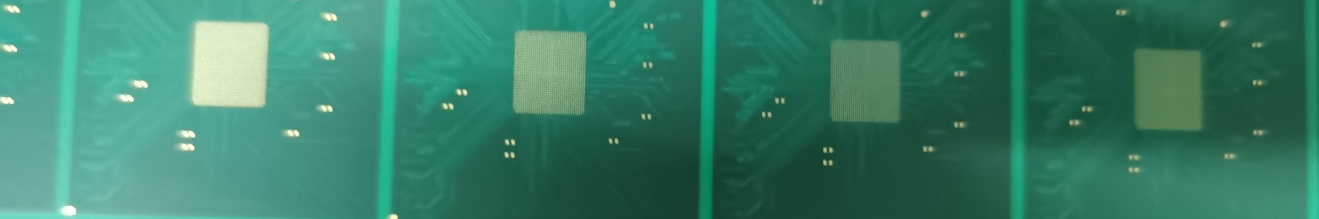
高周波PCB (HF プリント基板) are specialized printed circuit boards designed to handle high-frequency signals, typically in the range of 500 MHz to several GHz. These PCBs are essential in applications where signal integrity and minimal signal loss are crucial, such as in telecommunications, 航宇, 軍, and high-speed computing.
High-frequency signals can be significantly affected by the dielectric properties of the プリント基板 material, 信号経路のレイアウト, and environmental factors. Therefore, HF PCBs are made from materials with low dielectric constants (DKの) and low loss tangents (Dfの) to ensure minimal signal attenuation and distortion. Common materials used for HF PCBs include PTFE (Polytetrafluoroethylene), Rogers materials, and specialized high-frequency laminates.
The Types of High Frequency PCBs
High Frequency PCBs come in various types and configurations to meet the diverse needs of different applications. Some of the most common types include:
Single-Layer HF PCBs: These PCBs have a single conductive layer and are suitable for simple high-frequency circuits such as antennas and low-noise amplifiers. They offer easy fabrication and lower cost but limited functionality.
Multilayer HF PCBs: These PCBs consist of multiple layers of conductive materials separated by insulating layers. Multilayer HF PCBs are used in more complex applications where multiple high-frequency circuits need to be integrated into a compact space. They offer higher functionality and improved performance but are more complex to manufacture.
Hybrid HF PCBs: Hybrid HF PCBs combine high-frequency materials with traditional PCB materials to achieve specific performance characteristics. このアプローチにより、設計者はPCBのさまざまなセクションを最適化して、高周波性能とコスト効率を実現できます.
Flex and Rigid-Flex HF PCBs: These PCBs offer flexibility in design and are used in applications where the PCB needs to be bent or folded. They are commonly used in aerospace, 医療機器, およびウェアラブル電子機器.
The Advantages of High Frequency PCBs
High Frequency PCBs provide several advantages that make them indispensable in advanced electronic applications:
Superior Signal Integrity: HF PCBs maintain signal integrity by minimizing signal loss and distortion. This is crucial for high-speed data transmission and reliable performance in communication systems.
Low Dielectric Loss: The materials used in HF PCBs have low loss tangents, which reduce signal attenuation and ensure high-frequency signals can travel longer distances without degradation.
高い熱安定性: HF PCBs exhibit excellent thermal stability, allowing them to maintain performance and dimensional stability under high-temperature conditions, which is essential for high-power applications.
Mechanical Strength: These PCBs offer robust mechanical properties, enabling them to withstand the physical stresses encountered during assembly and operation.
Compatibility with Advanced Manufacturing Processes: HF PCBs are designed to be compatible with modern manufacturing processes, including automated assembly and high-precision fabrication techniques.
How to Design a High Frequency PCB?
Designing a High Frequency PCB requires careful consideration of various factors to ensure optimal performance. Here are the key steps in the design process:
Choose the appropriate high-frequency material based on the application requirements. Consider factors such as dielectric constant, loss tangent, thermal properties, and mechanical strength.
Maintain precise control over the impedance of transmission lines to ensure signal integrity. 電磁界シミュレーションソフトウェアを使用して、PCBトレースのインピーダンスをモデル化および検証します.
高周波信号パスの長さを最小限に抑えて、信号損失と干渉を低減. Use differential pair routing for high-speed differential signals to minimize crosstalk and electromagnetic interference.
堅牢な接地および配電ネットワークを設計して、安定した動作を確保し、ノイズを最小限に抑えます. Use ground planes to provide a low-impedance path for return currents.
効果的な熱管理戦略を取り入れる, サーマルビアやヒートシンクなど, ハイパワー部品から発生する熱を放散し、安定した動作を維持するため.
PCB設計が標準的な製造プロセスと互換性があることを確認します. PCBメーカーと緊密に連携して、設計パラメータと製造能力を確認します.
Why Use High Frequency PCBs Over Other Boards?
High Frequency PCBs offer distinct advantages over traditional PCBs in specific applications:
HF PCBs are designed to handle high-frequency signals with minimal loss and distortion, making them ideal for high-speed data transmission and communication systems.
The materials and construction techniques used in HF PCBs ensure high reliability and durability, even in harsh operating conditions.
HF PCBs can be customized to meet the specific performance requirements of advanced applications, such as aerospace, 軍, and high-speed computing.
High Frequency PCBs can be designed in various configurations, 単層を含む, 多層, ハイブリッド, and flex designs, to accommodate different application needs and form factors.
技術が進歩し、より高いデータレートと周波数に対する需要が高まるにつれて, HF PCBs provide a future-proof solution that can support emerging technologies and standards.
What is the High Frequency PCB Fabrication Process?
The fabrication process of High Frequency PCBs involves several critical steps to ensure high performance and reliability:
Select and prepare the high-frequency laminate material according to design specifications. 材料は必要な寸法にカットし、汚れを取り除くために洗浄する必要があります.
多層PCB用, 高温高圧下で個々の層をラミネートします. レイヤーの適切な位置合わせと接着を確認します.
設計レイアウトに応じたビアとコンポーネントリード用のドリル穴. 高周波信号の完全性を維持するためには、精密な穴あけが不可欠です.
ドリルで開けた穴とビアに銅をメッキして、レイヤー間に電気的接続を作成します. このステップにより、信頼性の高い信号伝送と機械的安定性が保証されます.
フォトリソグラフィーを使用して、回路パターンをラミネート材料に転写します. このプロセスでは、材料に感光性フィルムをコーティングします, マスクを通して紫外線を当てる, パターンの開発.
不要な銅をエッチングして、目的の回路パターンを明らかにします. このステップでは、正確でクリーンなトレースを確保するために、正確な制御が必要です.
表面仕上げを適用する, ENIGなど (無電解ニッケル浸漬金) または HASL (熱風はんだレベリング), 銅トレースを保護し、良好なはんだ付け性を確保するため.
電気試験と目視検査を実施して、PCBの性能と品質を確認します. これには、インピーダンス制御のチェックが含まれます, シグナルインテグリティ, そして全体的な機能性.
The Application of High Frequency PCBs
High Frequency PCBs are used in a wide range of advanced applications due to their superior performance and reliability:
HF PCBs are essential in wireless communication systems, 携帯電話を含む, 基地局, および衛星通信. 高速データ伝送と効率的な信号処理を可能にします.
HF PCBs are used in radar systems, 衛星ナビゲーション, 航空宇宙産業の通信機器. その優れた熱安定性と信頼性により、過酷な環境でも最適な性能を発揮します.
HF PCBs are employed in military communication systems, レーダー, および電子戦機器. 堅牢な構造と高性能により、ミッションクリティカルなアプリケーションに適しています.
HF PCBs are used in advanced driver-assistance systems (ADASの), レーダーセンサー, 現代の自動車における高速データ通信. 過酷な自動車環境でも信頼性の高い動作を保証します.
HF PCBs are used in servers, データセンター, and high-performance computing systems. They enable fast data transfer and processing, supporting the demands of modern computing applications.
よくあるご質問(FAQ)
What are the main advantages of High Frequency PCBs?
The main advantages include superior signal integrity, low dielectric loss, 高い熱安定性, mechanical strength, and compatibility with advanced manufacturing processes.
What application areas are suitable for High Frequency PCBs?
High Frequency PCBs are suitable for telecommunications, 航宇, 軍, automotive, and high-speed computing applications, とりわけ.
What is the difference between High Frequency PCBs and traditional PCBs?
High Frequency PCBs offer better signal performance, 信号損失の低減, and improved reliability in high-frequency applications compared to traditional PCBs, which are typically used for lower frequency and less demanding applications.
What factors should be considered when designing a High Frequency PCB?
考慮すべき要素には、材料の選択が含まれます, インピーダンス制御, 信号経路のレイアウト, 接地プレーンと電源プレーン, サーマルマネジメント, と製造可能性.
Is the fabrication process of High Frequency PCBs complex?
製造プロセスには、複数の正確なステップが含まれます, 材料の準備を含む, 積層, 錬成, 鍍金, パターン転送, エッチング, および表面仕上げ. 複雑ですが, これらの手順により、高品質で高性能なPCBが保証されます.


